Omron G6S-2G-12VDC: Footprint, Symbol, and 3D Model Guide
When integrating the Omron G6S-2G-12VDC relay into PCB designs, having precise footprint, symbol, and 3D models is essential for reliable manufacturing and visualization. In my experience, sourcing verified data, creating accurate custom models, and leveraging AI tools like Tripo can dramatically speed up and improve the design process. This guide details my practical approach to obtaining, building, and integrating these assets, with a focus on efficiency and real-world compatibility for engineers, PCB designers, and 3D modelers.
Key takeaways
- Verified footprints and symbols are crucial for error-free PCB layouts.
- Custom 3D modeling ensures mechanical fit and visual clarity in assemblies.
- AI-powered platforms like Tripo significantly streamline relay model creation.
- Always verify imported models for alignment, pin mapping, and scale.
- Optimize models for both ECAD and MCAD workflows to prevent integration issues.
- Troubleshoot common pitfalls early to avoid downstream manufacturing errors.
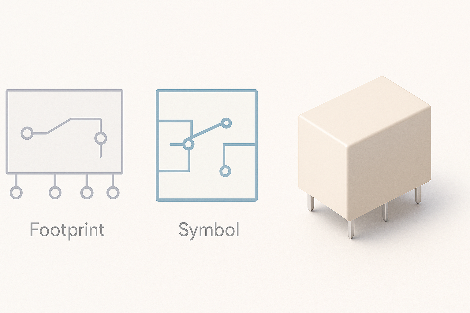
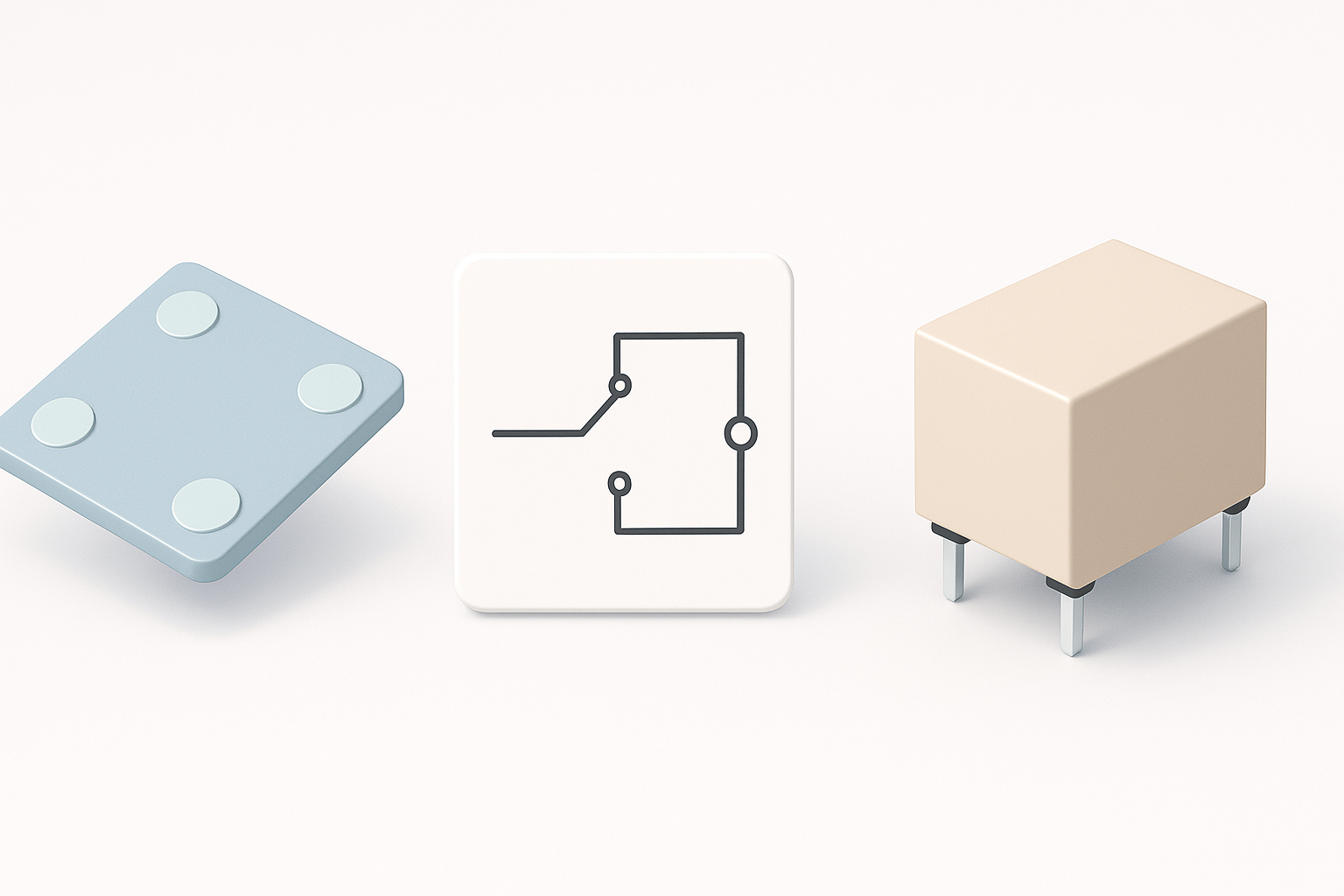
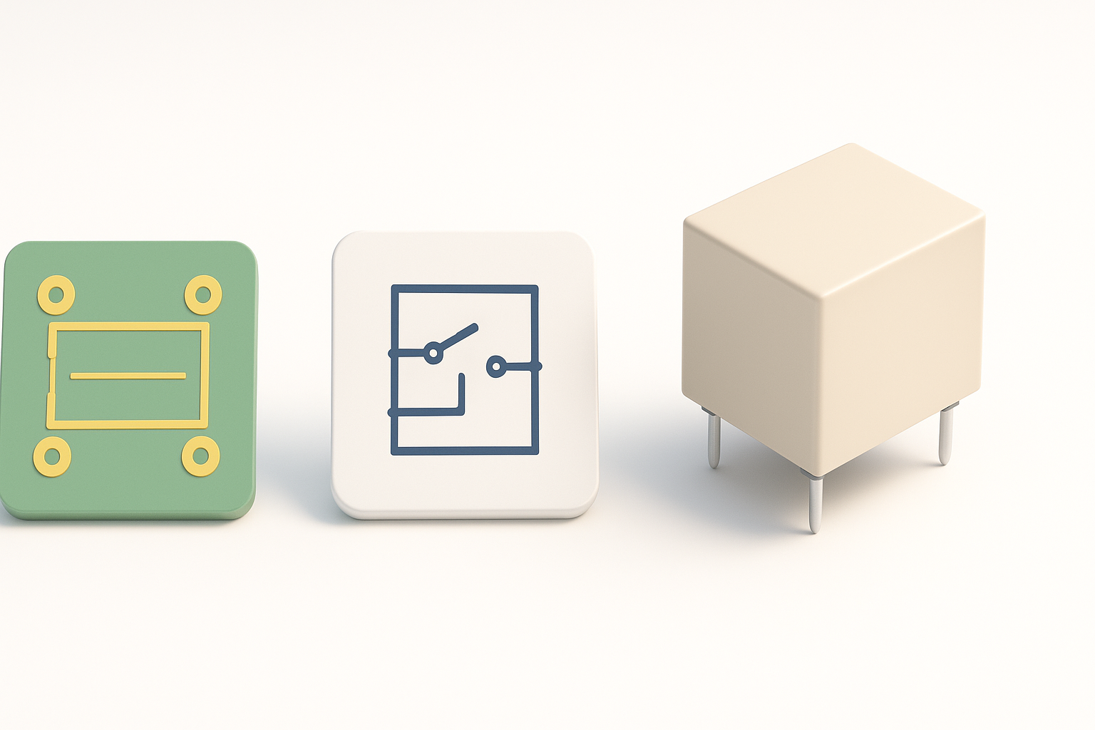
Understanding the Omron G6S-2G-12VDC Relay
Key specifications and applications
The Omron G6S-2G-12VDC is a compact, low-profile signal relay commonly used in telecom, instrumentation, and control systems. It features a 12V DC coil, dual-pole double-throw (DPDT) contacts, and a small footprint ideal for dense PCB layouts.
- Coil Voltage: 12V DC
- Contact Configuration: DPDT (2 Form C)
- Typical use cases: Signal switching, isolation, and compact relay banks
Why accurate models matter in design
Accurate footprints and symbols prevent layout errors and miswiring, while precise 3D models help catch mechanical clashes and aid in enclosure design. In my projects, using verified models has reduced prototype rework and improved collaboration between electrical and mechanical teams.
- Checklist:
- Confirm pin numbering and spacing
- Validate relay height and keepout zones
- Ensure 3D model matches datasheet dimensions
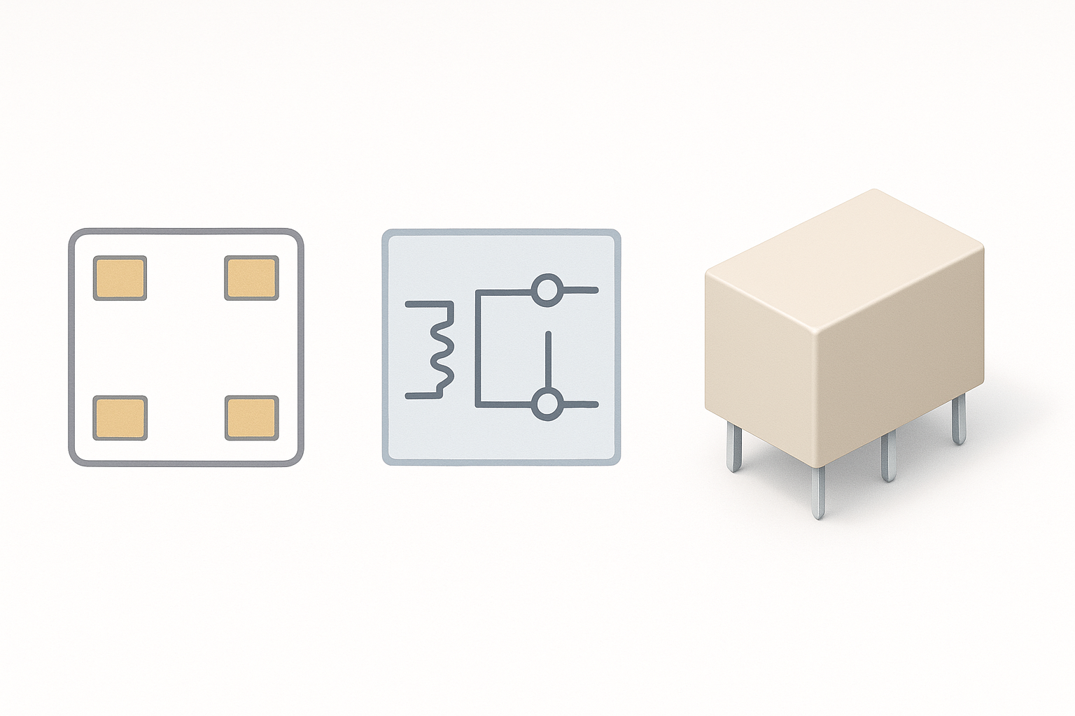
Obtaining and Creating the Footprint and Symbol
Where to find verified footprint and symbol data
I typically start by checking the manufacturer’s datasheet and reputable ECAD libraries. Many relay footprints and symbols are available from community repositories or directly from EDA tool plugins.
- Sources I trust:
- Manufacturer’s official CAD libraries
- Well-maintained ECAD community sites
- EDA tool built-in symbol/footprint wizards
My workflow for custom footprint and symbol creation
When data isn’t available or needs tweaking, I build custom assets:
- Footprint:
- Extract pad layout from datasheet
- Draw outline, pads, and silkscreen in EDA tool
- Double-check pin 1 orientation and mechanical cutouts
- Symbol:
- Map relay’s electrical function to schematic symbol
- Assign correct pin numbers and names
- Add logical grouping for clarity
Pitfalls:
- Mixing up pin order (especially for DPDT relays)
- Ignoring recommended pad sizes for soldering reliability
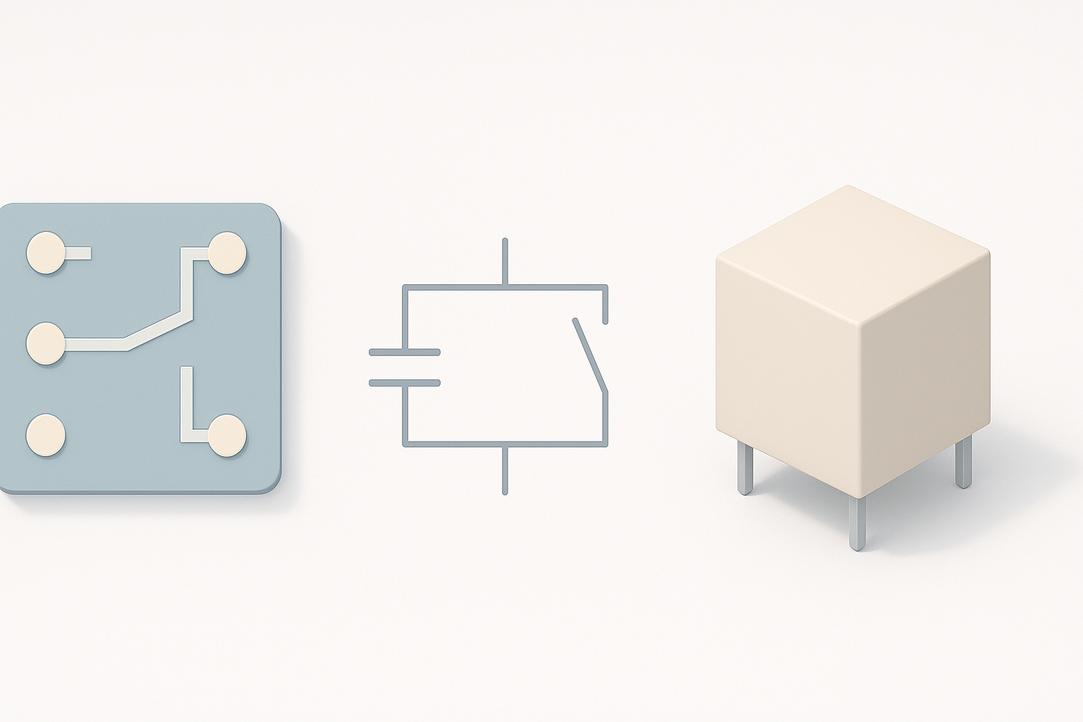
3D Modeling the Omron G6S-2G-12VDC Relay
Step-by-step process for building a 3D model
When a 3D model isn’t available, I build one using parametric modeling or AI-assisted tools like Tripo:
- Gather dimensions:
- Reference mechanical drawings from datasheet
- Note pin locations, body size, and standoff heights
- Model the body:
- Start with the main cuboid shape
- Add pin protrusions and chamfers
- Detailing:
- Model pin geometry for accurate PCB fit
- Add marking or branding if needed
- Export:
- Save in STEP or STL for ECAD/MCAD use
Best practices for accuracy and compatibility
- Align the model’s origin with the footprint’s pin 1 for seamless placement.
- Scale check: Ensure units match your PCB software (mm vs. inch).
- Simplify geometry to reduce file size without losing critical detail.
Pro tip: I always cross-check the finished model against the physical component before sign-off.
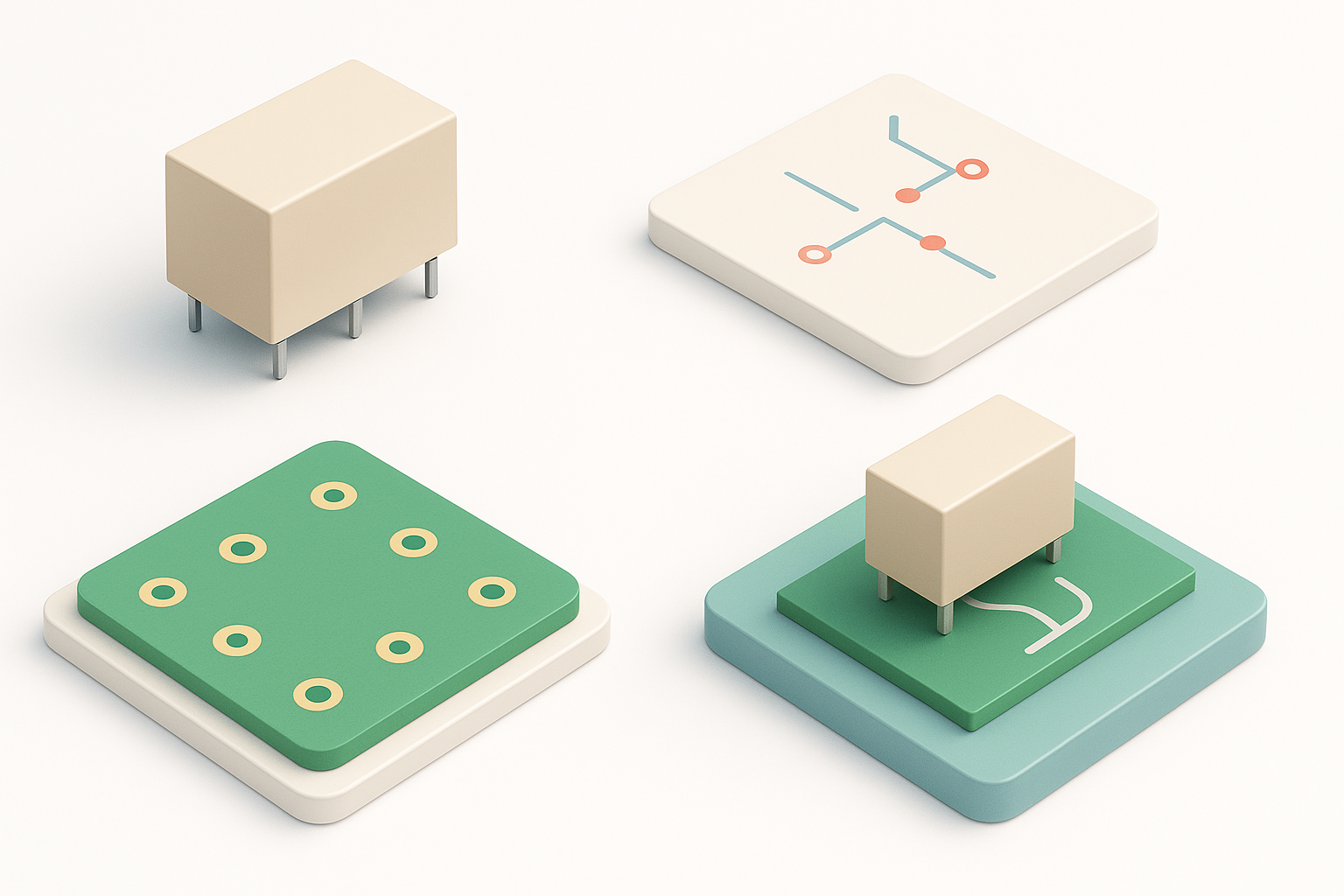
Integrating Models into PCB and CAD Workflows
Importing and verifying models in EDA software
Importing models can introduce alignment or scaling issues. My routine:
- Import the 3D model into the EDA tool’s footprint editor
- Verify pin positions align with pad locations
- Rotate and translate as needed for perfect fit
Checklist:
- Pin 1 orientation matches schematic
- No model overhangs outside board edge
- Height and keepout zones respected
Tips for seamless integration with 3D and ECAD tools
- Use neutral 3D formats (STEP, IGES) for cross-compatibility.
- Group relay body and pins as separate layers for easier editing.
- Regularly update your library to avoid model drift between projects.
Pitfall: Overly complex models can slow down 3D rendering—simplify where possible.
Leveraging AI Tools for Efficient 3D Model Creation
How I use Tripo AI for relay modeling
Tripo AI accelerates the modeling process, especially for standard components like relays:
- Upload datasheet or a clear photo/sketch
- Specify key dimensions and pin layout
- Let the AI generate a base model, which I then tweak for details
This approach typically saves me 30–50% of modeling time, especially for parts with repetitive geometry.
Comparing AI-driven and manual modeling approaches
- AI-driven:
- Faster initial results
- Good for standard shapes and quick iterations
- May need manual refinement for intricate details
- Manual modeling:
- Full control over every feature
- Necessary for highly custom or non-standard components
- More time-intensive
My advice: Use AI tools for rapid prototyping, but always validate output before release.
Troubleshooting and Optimization Tips
Common issues and how I resolve them
- Misaligned pins: Adjust model origin or pad mapping in the EDA tool.
- Wrong scale: Double-check units on import/export.
- Visual glitches: Simplify model geometry, remove unnecessary faces.
Quick fixes:
- Re-import with correct units
- Use EDA tool’s 3D preview to catch errors early
Optimizing models for manufacturing and visualization
- Strip unnecessary internal geometry to reduce file size.
- Use color coding or textures for easier assembly identification.
- For manufacturing, ensure model tolerances match PCB fab requirements.
Final tip: Regularly review and update your model library to incorporate feedback from assembly and manufacturing teams.
By following these strategies, I consistently deliver reliable and manufacturable PCB designs with accurate relay models—minimizing surprises during prototyping and production.


